


Explanation of Diode and power diode
Diodes are made with semiconductors such as silicon and
germanium.
Silicon has a crystalline structure. It has four
valence electrons forming valence bonds. Atoms share these electrons and they
are in the valence band and cannot move freely into the Cristal.
That is pure or intrinsic silicon. Adding impurities
change the conductive properties of silicon. This process is called doping.
There are two types of impurities:
Donors-it has five electrons in the outer shell.
(phosphorus, lithium, antimony, arsenic, and bismuth)
Acceptors- it has three electrons in the outer shell.
(boron, indium, nitrogen, aluminium, and gallium)
There are 2 types of semiconductors:
N-type doping with donors there is extra electrons
that can move around.
P-type doping with acceptors electron is missing in the
valence shell, we can observe as the positively charged hole.
PN junction is formed when P-type and N-type
semiconductors are put together physically. There is a diffusion of electrons
from N-type to the P-type side of the junction. This creates a +ly charged
region at the N-type side and -ly charged region at the P-type side.
This region is named depletion region and an electrical field is made which doesn't
allow additional electrons and holes to cross to the opposite side.
When PN junction is connected to voltage source there
are two different situations:
Forward
bias:
N-type region (cathode) connected to the negative pole
of source and P-type region (anode) connected to the positive pole – a large electric field is generated in the opposite direction. Depletion region becomes
narrower, electrons and holes can pass and current flows. This known as PN
junction is forward biased.
Reverse
bias:
N-type region (cathode) connected to the positive pole
of source and P-type region (anode) connected to the negative pole – a large
electric field is generated in the same direction. The depletion region becomes
wider. Electrons and holes cannot pass and the currents do not flow. This known
as PN junction is reverse biased.
What is a diode?
A diode is an electronic component with two terminals
called the anode and the cathode. The diodes are made with semiconductor
materials like silicon, germanium, or selenium. The main property of a diode is
its tendency to conduct current in just one direction.
What Is An Ideal Diode?
An ideal diode is zero resistance when it is forward biased
and infinite resistance when reverse biased.
What is a power diode?
The doping level of both P side N side is that the same
and hence we get a PN junction within the signal diodes but in power diodes,
we have a junction formed between a heavily doped P(positive) and a lightly
doped N(negative)layer which is epitaxially grown on a heavily doped N+ layer.
The N– layer is that the key feature of the facility
diode which makes it suitable for top power applications. This layer is
extremely lightly doped, almost intrinsic and hence the device is additionally
referred to as PIN diode.
What will happen if the voltage increase continuously in reverse bias?
If reverse applied voltage continuously increases it
then after a certain applied voltage the depletion layer will be destroyed. It
will cause a huge reverse current to flow through the diode.
If this current is not externally limited and it reaches
beyond the safe value, the diode may be permanently destroyed this is because as
a magnitude of the reverse voltage increases.
The current can be blocked by a diode when the applied
reverse voltage is less than a rated or specified voltage.
How to limit forward current in diode?
Forward current is limited by can add the external
resistance connected in series with the diode.
What is forward biased voltage in diode?
When the forward applied voltage is more than the barrier
potential of the junction voltage at which the forward current just starts to
flow is called forward-biased voltage and it is equal to the barrier potential
for silicon diode it is 0.7 volts for germanium diode it is 0.3 volts.
What is the forward-biased voltage for silicon?
Silicon forward biased voltage is around 0.7 volts.
What is the forward-biased voltage for germanium?
Germanium forward biased voltage is around 0.3 volts.
What Are the Two Mechanisms of Breakdown PN Junction diode?
Zener and avalanche breakdown.
What do you mean by break down voltage?
At which voltage an insulator to become conductive,
this voltage called the breakdown voltage.
What Is Reverse Saturation Current?
Reverse Saturation Current is a very small amount of
current which flows through the diode when the diode is reverse biased. Reverse
saturation current may be quite a leakage current or unwanted current. This
saturation current is caused by when the temperature increases of minority
carriers.
What is the difference between the diode and a power diode?
Design: power diodes are large heavy and typically have
metal shielding.
Voltage Rating: Power diodes have more voltage ratings
over a normal diode
.
Current Rating: Power diodes have high current ratings
over a normal diode.
Temperature: Power diodes designed for operation at a
higher temperature.
Cost: Power Diodes are costly.
What is the knee voltage of a forward-biased in PN junction diode?
Knee voltage is that the PN junction characteristics of
voltage. Silicon Knee voltage is about 0.6–0.7 V and 0.2–0.3 for Germanium.
The shape of the forward bias of the PN junction
characteristics curve seems like a knee, so it’s called knee voltage.
What is the difference between break down voltage and knee voltage?
The knee voltage: In the forward bias, the voltage at
which the current through the PN junction starts increasing rapidly is known as
knee voltage. It is also referred to as cut-in-voltage or threshold voltage.
Breakdown voltage: In the reverse bias the reverse the voltage at which the PN junction breakdown occurs is called a breakdown
voltage.
How do identify terminals of a conventional diode?
(Or)
How
can identify a diode which has no markings on it?
(Or)
How
do identify the negative and positive of a Zener diode?
If the diode does not have any markings on it than the
easiest way by using a Digital Multimeter on the diode scale.
Connect the positive (red) probe to the one terminal
and common (black) probe to the other terminal of the diode. Check the
multimeter if open circuit (OL) means diode is connected in reverse bias. So
black and red probes reference to anode and cathode.
Connect the positive (red) probe to the one terminal
and common (black) probe to the other terminal of the diode. Check the
multimeter if it will show some value, usually between 0.3 to 0.7 means diode
is connected in forward bias. So black and red probes reference to the cathode
and anode.
How do you identify a diode through a look?
A diode is a cylindrical shape widely, the silver band
marking side is known as the cathode. The diode is a two-terminal device.
Transparent cylindrical shape denotes Zener diode. The Zener breakdown voltage
is written on the diode.
How
do identify a diode whereas it is Zener diode or not?
We can identify by the physical look of the diode.
Zener diode shape is like a transparent cylindrical. The Zener breakdown
voltage is written on the diode and it is a two-terminal device.
How can know the voltage rating on a Zener diode?
- it’s normally written on the Zener diode, perhaps encoded in the part number.
- Check with part number and datasheet
- by bench test
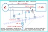
Where does the extra voltage go in the Zener diode?
or
What
happens when loading current changes in Zener diode?
For overvoltage protection from a Zener diode, it must
have a series resistor that will drop the excess current. When the Zener is not
conducting there will be no current through the series resistor because there
will be no current through the Zener. No current means no voltage drop across
this resistor. If the voltage exceeds the Zener breakdown then there will be
current through the series resistor and a voltage drop equal to the difference
between the applied voltage and the Zener breakdown.
What causes a Zener diode to fail?
In the Zener diode If the current through exceeds
beyond the rated current of the device and it will lead to heat loss. The heat
loss of the diode will permanently damage the diode.
What is the difference between a PN junction diode and a Zener diode?
The PN Junction diode is not designed for large reverse
bias voltage but Zener Diode is mainly designed for use in reverse bias
condition.
PN Junction Diodes are lightly doped but Zener diodes
are highly doped.
Can we use Zener diodes in a rectifier ckt?
Yes, we can use the Zener diode in rectifier ckts. But
we have to keep I/P voltage less than the Zener breakdown voltage, otherwise,
it will lead the short when I/P voltage goes above the breakdown voltage.
Should be I/P voltages is half of Zener breakdown voltage.
What are the difference between an avalanche breakdown and a Zener breakdown?
Zener break down is due to the following
characteristics
1 p-n junction is heavily doped
2. The depletion layer width is narrow
3. The potential barrier is low
4. The electric field is produced in strongly
5 Zener breakdown voltage is reduced when the
temperature increases
6. Zener breakdown voltage is normally lower than an
avalanche breakdown voltage
7. Zener breakdown due to the high electric field
Avalanche breakdown
1 p-n junction is lightly doped
2. The depletion layer width is wider
3. The potential barrier is high
4. There is not strong Electric field is produced
5. Avalanche breakdown voltage is increased when the
temperature increases
6. It is normally higher than the Zener breakdown
voltage.
7. Avalanche breakdown due to the collision of the
electrons, whereas the Zener breakdown occurs because of the high electric
field.
Types of Diodes:
- Light-emitting diode LED
- Photodiode
- Zener Diode
- Laser Diode
- Tunnel Diode
- Schottky Diode
- Vricap
- Transient voltage suppression diode
"It is not that life ashore is distasteful to me. But life at sea is better."
— Sir Francis Drake, Sea Captain


4 Comments
Uininliebi-Garland Tony Abbott https://wakelet.com/wake/_tjF3o7UBR4S3r89kdW8D
ReplyDeletetranconfive
morrgnosOsterne Lisa Parker Crack
ReplyDeleteranehorre
deptioad-gu2001 Lori Nance Nulled
ReplyDeleteScreenHunter Pro
DesignCAD 3D Max
tersdediscse
Visit For Best Seo Tool Website
ReplyDeleteWe love to hear your comments on this article, so that we may better serve you in the future.